The high resolution and contrast required in X-ray scintillation imaging is achieved using high-contrast imaging transducers made by coating a substrate with a rare earth metal, such as doped caesium iodide (CsI) wherein thallium (Tl) is often selected as the dopant.
The doped CsI coating is typically deposited onto the substrate using physical vapour deposition (PVD), forming a 100-600µm-thick film with columnar crystals having diameters of about 4-12µm. Each columnar crystal serves as a waveguide, trapping and guiding the X-ray scintillated light axially along its length. A moisture barrier such as Parylene with a thickness of about 5-30µm is usually applied over the coating, enhancing its durability.
The coated substrate provides a scintillation layer converting incident X-rays to an optical image that is subsequently transferred to an imaging device, such as a charged couple device. The CsI film serves as the ‘active’ X-ray sensitive scintillator and the substrate provides both mechanical support to the CsI film and acts as either a means to guide scintillated light to the imaging device, or as a back-reflect or light absorber. The thicknesses of conventional substrates can make it difficult to manufacture thin scintillation elements.
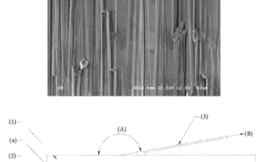
In February 2020, Scintacor Ltd was granted UK patent GB2570058B titled Caesium iodide (CsI) materials, which discloses a method of producing a CsI film (1) comprising the steps of (i) providing a substrate (3) comprising a layer of flexible material having a surface, (ii) forming a layer of CsI onto said surface of the flexible material, (iii) removing the layer of flexible material from the CsI layer to provide a CsI film, wherein prior to step (iii) the CsI-coated flexible material is place CsI-side down on a flat surface (2). Optionally, the layer of flexible material is removed by peeling the material from the CsI layer.
The substrate may be aluminium, copper, or a polymer, such as the polyimide film Kapton, and may provide sufficient flexibility to enable its separation and removal from the CsI layer by peeling under ambient conditions. Thus, the invention provides a free-standing CsI film, independent of a supporting substrate that is mechanically coherent allowing it to be handled. Optionally, the CsI-coated substrate may be transferred to a vacuum chamber, prior to peeling, for applying a barrier film/protective layer (4) on the CsI film (not in contact with the flexible layer). The substrate may be peeled at an angle (A) of about 120-180° in a direction (B) with respect to the CsI-deposited layer, such that little or no damage is imparted to the underlying CsI layer.
In one example, an aluminium foil substrate was coated using a layer of Tl-doped CsI via PVD, with conditions chosen to achieve the desired columnar growth to a target depth of 150µm. A 10µm-thick Parylene film was applied in a vacuum chamber to form a transparent humidity barrier. The CsI-coated substrate was placed CsI-side down on a flat surface and the aluminium foil substrate was peeled back at an angle of ~170° and completely separated to form a free-standing CsI film.
The invention allows for the use of a wide range of substrates and CsI films with a lower frequency of localised disrupted growth. Further, the patented method may allow for CsI films having much larger surface areas as compared with those made using conventional techniques. The free-standing film may be suitably coupled with an imaging device with either one of its sides facing in the direction of operation. In addition, the CsI film may be directly attached to a sensor or be used in applications where some flexural compliance is desirable, and devices may also benefit from the omission of the substrate e.g. due to reduced X-ray absorbance.
Read the full patent here
This article first appeared in the June 2020 issue of Materials World, the member magazine of the Institute of Materials, Minerals and Mining.


